- 您现在的位置:买卖IC网 > Sheet目录1992 > DS1010S-50+T&R (Maxim Integrated Products)IC DELAY LINE 10TAP 16-SOIC
DS1010
3 of 6
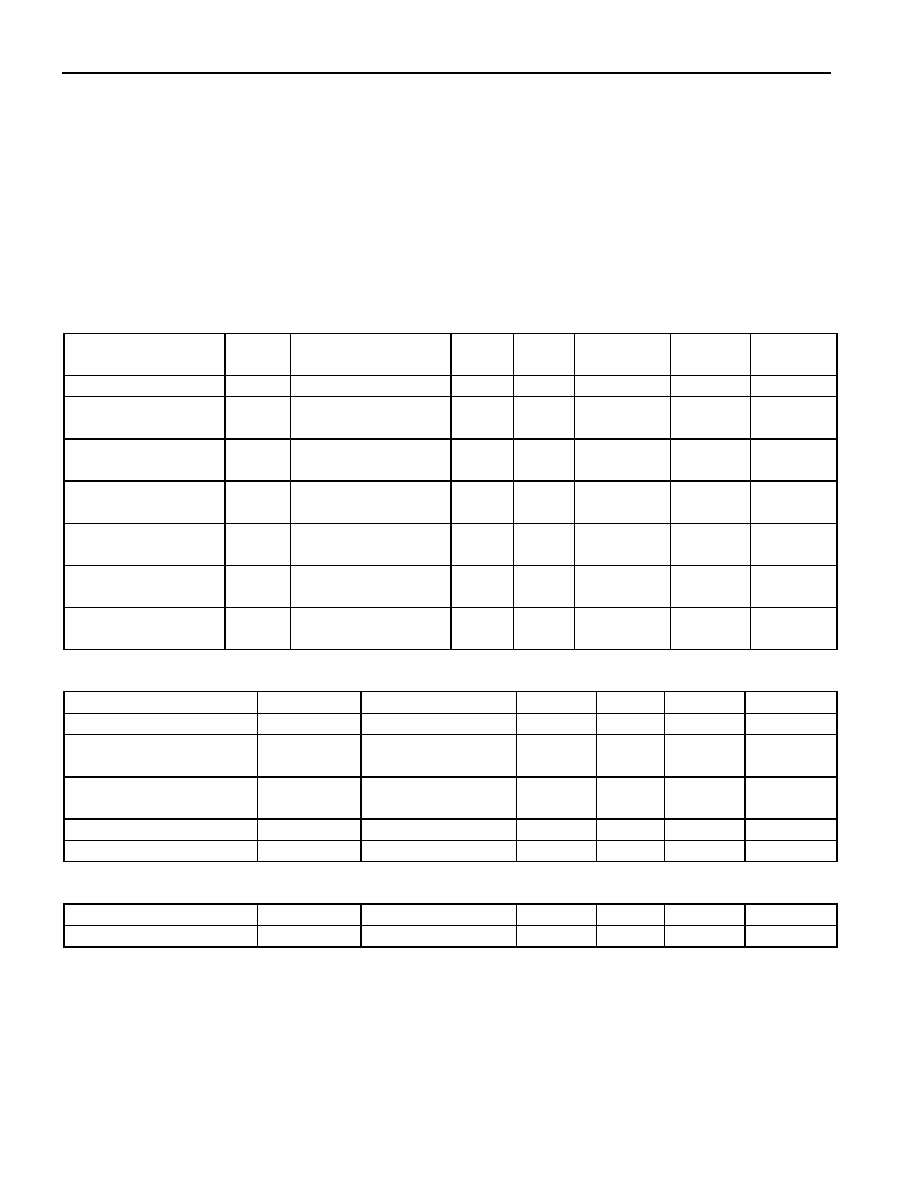
ABSOLUTE MAXIMUM RATINGS*
Voltage on Any Pin Relative to Ground
-1.0V to +7.0V
Operating Temperature
0
°C to 70°C
Storage Temperature
-55
°C to +125°C
Soldering Temperature
260
°C for 10 seconds
Short Circuit Output Current
50 mA for 1 second
* This is a stress rating only and functional operation of the device at these or any other conditions above
those indicated in the operation sections of this specification is not implied. Exposure to absolute
maximum rating conditions for extended periods of time may affect reliability.
DC ELECTRICAL CHARACTERISTICS
(0°C to 70°C; VCC = 5.0V ± 5%)
PARAMETER
SYM
TEST
CONDITION
MIN
TYP
MAX
UNITS
NOTES
Supply Voltage
VCC
4.75
5.00
5.25
V
1
High Level Input
Voltage
VIH
2.2
VCC + 0.5
V
1
Low Level Input
Voltage
VIL
-0.5
0.8
V
1
Input Leakage
Current
II
0.0V
≤ V
I
≤ V
CC
-1.0
1.0
A
Active Current
ICC
VCC=Max;
Period=Min.
40
150
mA
2
High Level Output
Current
IOH
VCC=Min.
VOH=4
-1.0
mA
Low Level Output
Current
IOL
VCC=Min.
VOL=0.5
12
mA
AC ELECTRICAL CHARACTERISTICS
(TA = 25°C; VCC = 5V ± 5%)
PARAMETER
SYMBOL
MIN
TYP
MAX
UNITS
NOTES
Input Pulse Width
tWI
40% of TAP 10 tPLH
ns
8
Input to Tap Delay
(leading edge)
tPLH
Table 1
ns
3, 4, 5, 6,
7, 9
Input to Tap Delay
(trailing edge)
tPHL
Table 1
ns
3, 4, 5, 6,
7, 9
Power-up Time
tPU
100
ms
Period
4 (tWI)ns
8
CAPACITANCE
(TA = 25°C)
PARAMETER
SYMBOL
MIN
TYP
MAX
UNITS
NOTES
Input Capacitance
CIN
510
pF
发布紧急采购,3分钟左右您将得到回复。
相关PDF资料
DS1013S-25+T&R
IC DELAY LINE 25NS 16-SOIC
DS1020S-50+T
IC DELAY LINE 256TAP 16-SOIC
DS1021S-50+T&R
IC DELAY LINE 256TAP 16-SOIC
DS1023S-25+W
IC DELAY LINE 256TAP 16-SOIC
DS1033Z-8+W
IC DELAY LINE 8NS 8-SOIC
DS1040Z-D70+
IC DELAY LINE 5TAP 70NS 8-SOIC
DS1044R-10+T&R
IC DELAY LINE 10NS 14-SOIC
DS1045S-4+T&R
IC DELAY LINE 16TAP 16-SOIC
相关代理商/技术参数
DS1010S-500
功能描述:延迟线/计时元素 RoHS:否 制造商:Micrel 功能:Active Programmable Delay Line 传播延迟时间:1000 ps 工作温度范围: 封装 / 箱体:QFN-24 封装:Tube
DS1010S-500/T&R
功能描述:延迟线/计时元素
RoHS:否 制造商:Micrel 功能:Active Programmable Delay Line 传播延迟时间:1000 ps 工作温度范围: 封装 / 箱体:QFN-24 封装:Tube
DS1010S-60
功能描述:延迟线/计时元素
RoHS:否 制造商:Micrel 功能:Active Programmable Delay Line 传播延迟时间:1000 ps 工作温度范围: 封装 / 箱体:QFN-24 封装:Tube
DS1010S-60/T&R
制造商:Maxim Integrated Products 功能描述:IC DELAY LINE 10TAP 60NS 16SOIC
DS1010S-60/T&R
功能描述:延迟线/计时元素
RoHS:否 制造商:Micrel 功能:Active Programmable Delay Line 传播延迟时间:1000 ps 工作温度范围: 封装 / 箱体:QFN-24 封装:Tube
DS1010S-75
功能描述:延迟线/计时元素
RoHS:否 制造商:Micrel 功能:Active Programmable Delay Line 传播延迟时间:1000 ps 工作温度范围: 封装 / 箱体:QFN-24 封装:Tube
DS1010S-75/T&R
功能描述:延迟线/计时元素
RoHS:否 制造商:Micrel 功能:Active Programmable Delay Line 传播延迟时间:1000 ps 工作温度范围: 封装 / 箱体:QFN-24 封装:Tube
DS1010S-80
制造商:未知厂家 制造商全称:未知厂家 功能描述:Tapped Delay Line